What is “Ryzen+” ZEN+?
After the very successful launch of the original “Ryzen” (Zen/Zeppelin – “Summit Ridge” on 14nm), AMD has been hard at work optimising and improving the design: “Ryzen+” (code-name “Pinnacle Ridge”) is thus a 12nm die shrink that can also includes APU – with integrated “Vega RX” graphics” – as well as traditional CPU versions.
While new chipsets (AMD 400 series) will also be introduced, the CPUs do work with existing AM4 300-series chipsets (e.g. X370, B350, A320) with a BIOS/firmware update which makes them great upgrades.
Here’s what AMD says it has done for Ryzen+:
- Process technology optimisations (12nm vs 14nm) – lower power but higher frequencies
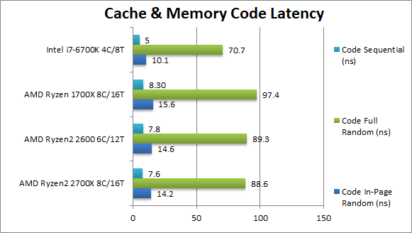
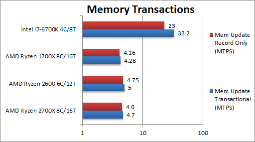
- Improvements for cache & memory speed & latencies (we are testing them in this article!)
- Multi-core optimised boost (aka Turbo) algorithm – XFR2 – higher speeds
In this article we test CPU Cache and Memory performance; please see our other articles on:
Hardware Specifications
We are comparing the top-of-the-range Ryzen+ (2700X, 2600) with previous generation (1700X) and competing architectures with a view to upgrading to a mid-range high performance design.
| CPU Specifications | AMD Ryzen 2700X (Pinnacle Ridge) | AMD Ryzen 2600 (Pinnacle Ridge) |
AMD Ryzen 1700X (Summit Ridge) |
Intel i7-6700K (SkyLake) |
Comments | |
| L1D / L1I Caches (kB) |
8x 32kB 8-way / 8x 64kB 8-way | 6x 32kB 8-way / 6x 64kB 8-way | 8x 32kB 8-way / 8x 64kB 8-way | 4x 32kB 8-way / 4x 32kB 8-way | Ryzen+ data/instruction caches is unchanged; icache is still 2x as big as Intel’s. | |
| L2 Caches (kB) |
8x 512kB 8-way | 6x 512kB 8-way | 8x 512kB 8-way | 4x 256kB 8-way | Ryzen+ L2 cache is unchanged but we’re told latencies have been improved. And 4x bigger than Intel’s! | |
| L3 Caches (MB) |
2x 8MB 16-way | 2x 8MB 16-way | 2x 8MB 16-way | 8MB 16-way | Ryzen+ L3 caches are also unchanged – but again lantencies are meant to have improved. With each CCX having 8MB even the 2600 has 2x as much cache as an i7. | |
| TLB 4kB pages |
64 full-way 1536 8-way | 64 full-way 1536 8-way | 64 full-way 1536 8-way | 64 8-way 1536 6-way | No TLB changes. | |
| TLB 2MB pages |
64 full-way 1536 2-way | 64 full-way 1536 2-way | 64 full-way 1536 2-way | 8 full-way 1536 6-way | No TLB changes, same as 4kB pages. | |
| Memory Controller Speed (MHz) | 600-1200 | 600-1200 | 600-1200 | 1200-4000 | Ryzen’s memory controller runs at memory clock (MCLK) base rate thus depends on memory installed. Intel’s UNC (uncore) runs between min and max CPU clock thus perhaps faster. | |
| Memory Speed Rated/Max (MHz) |
2400 / 2933 | 2400 / 2933 | 2400 / 2666 | 2533 / 2400 | Ryzen+ how supports up to 2933MHz (officially) which should improve its performance quite a bit – unfortunately fast DDR4 is very expensive right now. | |
| Memory Channels / Width |
2 / 128-bit | 2 / 128-bit | 2 / 128-bit | 2 / 128-bit | All have 128-bit total channel width. | |
| Memory Timing (clocks) |
14-16-16-32 7-54-18-9 2T | 14-16-16-32 7-54-18-9 2T | 14-16-16-32 7-54-18-9 2T | 16-18-18-36 5-54-21-10 2T | Memory runs at the same timings on both Ryzen+ and Ryzen but we shall see if measured latencies are different. | |
Core Topology and Testing
As discussed in the previous article, cores on Ryzen are grouped in blocks (CCX or compute units) each with its own 8MB L3 cache – but connected via a 256-bit bus running at memory controller clock. This is better than older designs like Intel Core 2 Quad or Pentium D which were effectively 2 CPU dies on the same socket – but not as good as a unified design where all cores are part of the same unit.
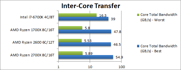
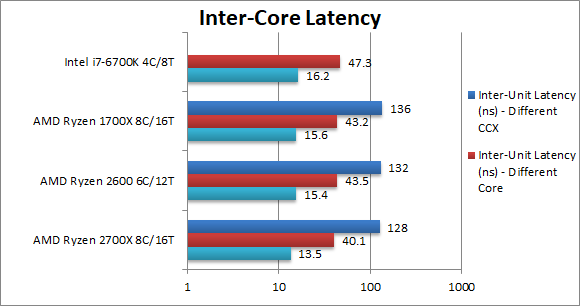
Running algorithms that require data to be shared between threads – e.g. producer/consumer – scheduling those threads on the same CCX would ensure lower latencies and higher bandwidth which we will test with presently.
We have thus modified Sandra’s ‘CPU Multi-Core Efficiency Benchmark‘ to report the latencies of each producer/consumer unit combination (e.g. same core, same CCX, different CCX) as well as providing different matching algorithms when selecting the producer/consumer units: best match (lowest latency), worst match (highest latency) thus allowing us to test inter-CCX bandwidth also. We hope users and reviewers alike will find the new features useful!
Native Performance
We are testing native arithmetic, SIMD and cryptography performance using the highest performing instruction sets (AVX2, AVX, etc.). Ryzen supports all modern instruction sets including AVX2, FMA3 and even more.
Results Interpretation: Higher rate values (GOPS, MB/s, etc.) mean better performance. Lower latencies (ns, ms, etc.) mean better performance.
Environment: Windows 10 x64, latest AMD and Intel drivers. 2MB “large pages” were enabled and in use. Turbo / Boost was enabled on all configurations.
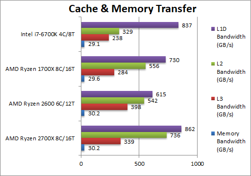
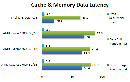
Ryzen+ brings nice updates – good bandwidth increases to all caches L1D/L2/L3 and also well-needed latency reduction for data (and code) accesses. Yes, there is still work to be done to bring the latencies down further – but it may be just enough to beat Intel to 2nd place for a good while.
At the high-end, ThreadRipper2 will likely benefit most as it’s going against many-core SKL-X AVX512-enabled competitor which is a lot “tougher” than the normal SKL/KBL/CFL consumer versions.
SiSoftware Official Ranker Scores
Final Thoughts / Conclusions
As with original Ryzen, the cache and memory system performance is not the clean-sweep we’ve seen in CPU testing – but Ryzen+ does bring welcome improvements in bandwidth and latency – which hopefully will further improve with firmware/BIOS updates (AGESA firmware).
With the potential to use faster DDR4 memory – Ryzen+ can do far better than in this test (e.g. with 2933/3200MHz memory). Unfortunately at this time DDR4 – especially high-end fast versions – memory is hideously expensive which is a bit of a problem. You may be better off using less but fast(er) memory with Ryzen designs.
Ryzen+ is a great update that will not disappoint upgraders and is likely to increase AMD’s market share. AMD is here to stay!

